(China (Mainland))

Product Summary
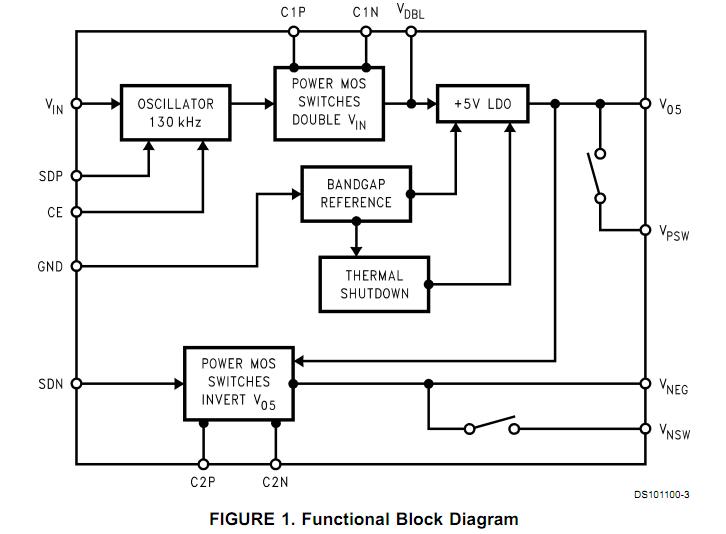
The LM2665M6X is a CMOS charge-pump voltage converter. It operates as an input voltage doubler, +5V regulator and inverter for an input voltage in the range of +2.85V to +6.5V. Five low cost capacitors are used in this circuit to provide up to 50mA of output current at +5V (± 5%), and 15mA at -5V. The LM2685MTC operates at a 130 kHz switching frequency to re- duce output resistance and voltage ripple. With an operating current of only 800μA (operating efficiency greater than 80% with most loads) and 6μA typical shutdown current, the LM2665M6X is ideal for use in battery powered systems. The device is in a small 14-pin TSSOP package. The applications of the LM2665M6X include Cellular phones, PDAs, Handheld instrumentation and 3.3V to 5V voltage conversion applications.
Parametrics
LM2665M6X absolute maximum ratings: (1)Supply Voltage (VIN to GND or GND to VNEG): 6.8V; (2)SDN, SDP, CE: (GND - 0.3V) to (VIN + 0.3V); (3)V05 Continuous Output Current: 80mA; (4)Continuous Power Dissipation (TA= 25℃): 600mW; (5)TJMAX: 150℃; (6)θJA: 140℃/W; (7) Operating Ambient Temp. Range: -40 to 85℃; (8) Operating Junction Temp. Range: -40 to 125℃; (9) Storage Temp. Range: -65 to 150℃; (10)Lead Temp. (Soldering, 10 sec.): 300℃; (11) ESD Rating: 2kV.
Features
LM2665M6X features: (1) +5V regulated output; (2) Inverts V05 (+5V) to VNEG (-5V); (3) Doubles input supply voltage; (4)TSSOP-14 package; (5)80% typical conversion efficiency at 25mA; (6)Input voltage range of 2.85V to 6.5V; (7)Independent shutdown control pins.
Diagrams
| Image | Part No | Mfg | Description |  |
Pricing (USD) |
Quantity | ||||||||||||
|---|---|---|---|---|---|---|---|---|---|---|---|---|---|---|---|---|---|---|
 |
 LM2665M6X |
National Semiconductor (TI) |
Charge Pumps |
Data Sheet |
|
|
||||||||||||
 |
LM2665M6X/NOPB |
National Semiconductor (TI) |
Charge Pumps |
Data Sheet |
|
|
||||||||||||