(China (Mainland))


Product Summary
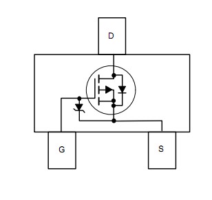
The FDV302P P-Channel logic level enhancement mode field effect transistor is produced using Fairchild proprietary, high cell density, DMOS technology. This very high density process is especially tailored to minimize on-state resistance. The FDV302P has been designed especially for low voltage applications as a replacement for digital transistors. Since bias resistors are not required, this one P-channel FET can replace several digital transistors with different bias resistors such as the DTCx and DCDx series.
Parametrics
FDV302P absolute maximum ratings: (1)Drain-Source Voltage: -25 V; (2)Gate-Source Voltag: -8 V; (3)Drain Current: Continuous, -0.12 A; Pulsed, 0.5; (4)Maximum Power Dissipation: 0.35 W; (5)Operating and Storage Temperature Range: -55 to 150℃; (6)Electrostatic Discharge Rating MIL-STD-883D Human Body Model (100pf / 1500 Ohm): 6.0 kV.
Features
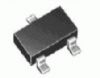
FDV302P features: (1)-25 V, -0.12 A continuous, -0.5 A Peak, RDS(ON) = 13 W @ VGS= -2.7 V; RDS(ON)= 10 W @ VGS = -4.5 V; (2)Very low level gate drive requirements allowing direct operation in 3V circuits. VGS(th) < 1.5V; (3)Gate-Source Zener for ESD ruggedness; (4)>6kV Human Body Model; (5)Compact industry standard SOT-23 surface mount package; (6)Replace many PNP digital transistors (DTCx and DCDx) with one DMOS FET.
Diagrams
| Image | Part No | Mfg | Description |  |
Pricing (USD) |
Quantity | ||||||||||||
|---|---|---|---|---|---|---|---|---|---|---|---|---|---|---|---|---|---|---|
 |
 FDV302P |
Fairchild Semiconductor |
MOSFET Digital FET P-Ch |
Data Sheet |
|
|
||||||||||||
|
FDV302P_D87Z |
Fairchild Semiconductor |
MOSFET Digital FET P-Ch |
Data Sheet |
Negotiable |
|
||||||||||||
|
FDV302P_NB8V001 |
Fairchild Semiconductor |
MOSFET Digital FET P-Ch |
Data Sheet |
|
|
||||||||||||
 |
FDV302P_Q |
Fairchild Semiconductor |
MOSFET Digital FET P-Ch |
Data Sheet |
Negotiable |
|
||||||||||||